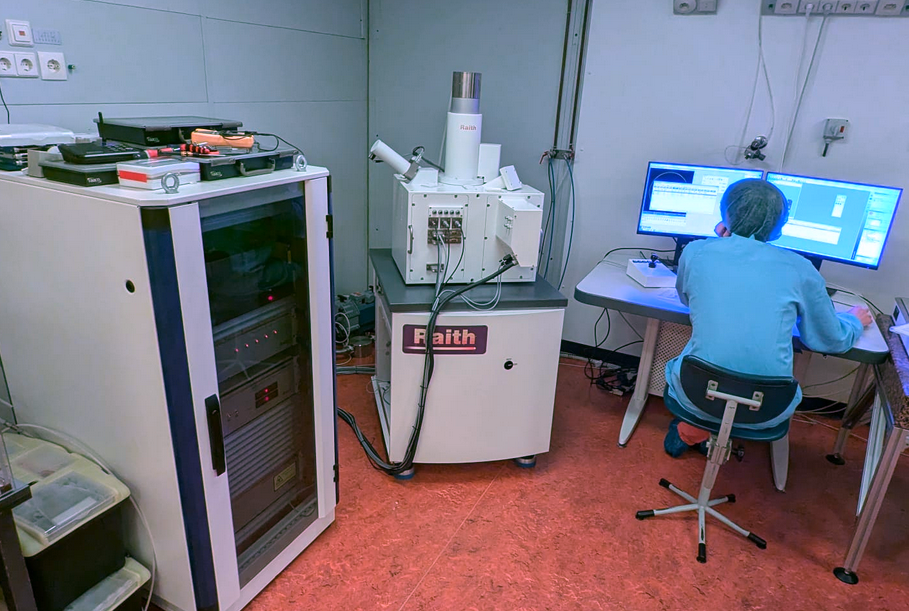
¶ Raith 100 E-beam EBPG
| Location | Cleanroom (HL612) |
|---|---|
| Functions | Electron beam lithography (>60 nm) |
| Specimen | ~ 15x15 mm samples, standard wafer thickness |
| Manufacturer | Tescan & Raith |
| Responsible | Luc Wigbout |
The Raith 100 is a direct-write machine used for maskless lithography. A 30 keV electron beam is emitted from a field-emitter, and is focused through electromagnetic lenses. Using a deflection system the beam can be moved in the xy-plane. Lithography is crucial for the planar process (i.e. fabrication of devices), since it is one of the techniques that allows local changes (along with, e.g. FIB and (F)EBID), whereas deposition and etching typically is a global step.
¶ The electron beam and writing fields
The Raith-100 e-beam lithography machine can be used to pattern nanoscale structures using an electron beam. The system is, in essence, an scanning electron microscope (SEM) with additional features such as a pattern generator that can write the desired patterns.
The e-beam is generated by thermionic emission from a hot cathode emitter at an energy of 30 keV, after which it is formed by the Wehnelt cylinder and several lenses (a.o. the stigmator and objective lens). Within the lens-column, there is also a deflector housed, which can change the incident angle of the electron beams. The amount of power necessary the deflect the 30 keV e-beam, increases with the beam angle. Thus, deflections at larger angles need bigger amplification. In the Raith-100, the large amplifiers tend to be noisy, so when writing, we will keep to the smaller amplification, so that the maximum angle corresponds to a field of view of 400x400 um.
The system can still be used as a SEM, were the electron beam is scanned across an area. The scanning movement is ‘locked-in’ with a detector such that an image can be created. The area that is imaged, is the field of view (FOV) at that specific magnification, e.g., at 575x mag., the FOV is 400x400 um and at 2300x mag., the FOV is 100x100 um. When writing, we typically use 100x100 um as the area of our writing fields (WF). Thus, the WF is the area onto which can be written by purely changing the deflection of the beam.
Since most patterns tend to be a bit larger than 100x100 um, we have to come up with creative solutions as not to write a noisy pattern. One way of overcoming this issue, is by stitching several WF's in two dimensions. This can be done by moving the sample with high accuracy.
¶ WF alignment
The sample is put onto a sample holder which can be mounted inside the Raith-100 onto a stage with sapphire ball spacers to ensure that it is held in place with extreme accuracy. Furthermore, the sample stage can be moved in X and Y directions. The movement is measured with a laser-interferometer.
By moving the stage 100 um along the X or Y axis, one could switch to another part on the sample. In order to make sure that all the WF’s are aligned--connect properly--a WF-alignment procedure has to be done. This procedure makes sure that all the writing fields are correctly stitched to each other.
WF alignment with images is done using an automated function, which does the following. After you searched for a particle or clear feature with a size of about 5 um, the procedure takes an image.
¶ Manual
¶ Preparations
Spin coat your resist of choice, see resist recipes at the respective resist page.
Non-conducting samples: If sample is non-conducting: spincoat (multiple) layers of conductive polymer (e.g. PEDOT or Electra92) or first deposit a conductive layer (if possible).
Check the sample under the optical microscope. Look for clean spots where you can write your pattern. Write down the coordinates of the good spots (Global CS).
On the PC, run the required software:
![]() VegaTC (SEM-software)
VegaTC (SEM-software)
![]() E-line (patterning software)
E-line (patterning software)
![]() Raith Protocol Tool (logging software)
Raith Protocol Tool (logging software)
And, if it is not open already, open the Logbook Excel-file (on the Desktop of the PC) to log the pressure upon walking in.
VegaTC: Vent the system and open the door by pulling carefully.
Exchange position: Be aware that when you (un)load the sample, the stage should be in the exchange position. Otherwise the mirrors of the interferometer could be exposed to the outer environment and potentially get dusty.
Mount the substrate on the sample holder as close as possible to the Faraday cup, so either slot 3 or 4.
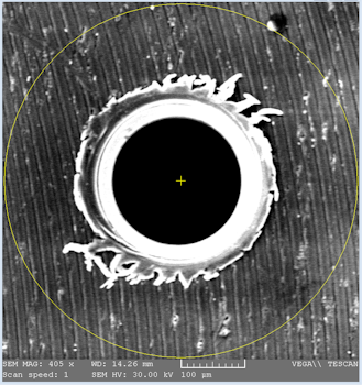
Make a scratch in the lower left corner of your substrate, about 1 mm in length, start on your sample and scratch outwards. Do not scratch as you would with lottery tickets, but make one swift scratch.
Mount the sample holder in the system, be careful; the sample holder is fixed with ceramic parts.
Carefully close the door.
VegaTC: Pump down the chamber. You need to push the door a bit to make a tight seal, as soon as the sound of the pre-pump gets softer and you see the pressure in the chamber drop, you can let go.
E-line: Open your design and, if not already open, open wafermap (File > Open wafermap > c:/eline/allusers/wafer/100mm _ush.wlo)
Wafermap navigation: You can use the wafermap to click where the stage should move. With CTRL right click the stage moves such that that position is underneath the objective lens. (This is useful when you want to navigate close to the origin or when doing 3-point alignment.) CTRL left click will point to a feature to do an alignment. This can be used during manual writefield alignment.
¶ Setting up the e-beam
VegaTC: Check that the selected voltage is 30kV.
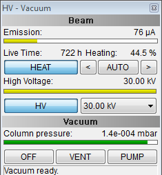
VegaTC: Turn on HV when pressure is <9.9 E-5 mbar. The emission current should be around 60-90 uA. If the emission current remains 0 uA after turning the HV on, do not be alarmed (yet). The system has a specific filament current that can be set, and sometimes this current needs to be higher in order to have emission. If the emission is 0 uA when the HV is on, click on AUTO in the 'HV - Vacuum' panel ( < AUTO > ), this will perform an automatic heating procedure. If this procedure does not fix the emission, check what its lifetime is: if it is close to 1000 hours, contact the responsible technician for a replacement.
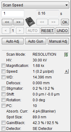
VegaTC: Check in the SEM-image that there is a yellow cross in the center. If not, make it appear by going to: Extensions > Measurements. Choose a radial grid with 63.04 um spacing.
E-line: Check that the PAT/IMG button is working by pressing  /
/  .
.
E-line: Also make sure beam blanker is working by pressing  /
/  .
.
Leave the beam blanked for now to prevent accidental exposure of your sample!
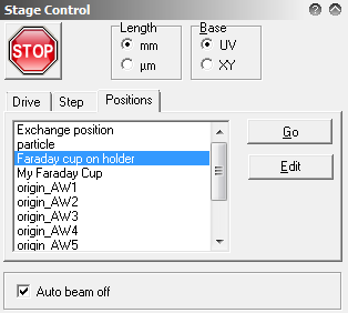
E-line: On the right panel, open the Adjustments pane by clicking  . In the Stage Control window, select
 Faraday cup holder and press Go. Once you are there, unblank the beam. If you see nothing, zoom out in the VegaTC software.
If the Faraday cup isn't centered correctly all beam current measurements will be off.
Center the Faraday cup by moving the stage with the joystick on the desk. Once it is centered, click Faraday cup on holder > Edit > Read, this will save the current position of the stage to the the Faraday cup.
VegaTC: Choose the PC you will be using by clicking the text 'PC' (NOT the checkbox!) and changing the value in the top left.
E-line: Measure the beam current. In the table you can find typical values for the beam current. If the beam current is low you can perform an automatic heating procedure (see above).
| PC | Typical beam current | Spot size | Use case |
|---|---|---|---|
| 1 | 10 nA | 690 nm | Contact pads |
| 5 - 9 | 0.3 - 1.3 nA | (Hardly used) | |
| 10 | 0.150 nA | 87 nm | Typical features |
| 12-14 | 0.05 nA | 34-52 nm | High resolution |
¶ Origin correction
Define the origin of the global coordinate system on your sample. Typically this is the lower left corner.
E-line: Press CTRL + right click on the wafermap where you expect the origin of the sample to be, aim a little bit below to make sure you don't expose your sample.
VegaTC: Once the stage has moved to the position you selected, carefully zoom out and look for the origin, slowly moving towards it. As soon as you see it, zoom in a bit to leave the sample as much out of the FOV to make sure you do not prematurely expose your resist by accident. Keep sample origin in upper right corner of image window to avoid exposing the sample. Keep zooming in and use the joystick to move the stage, keep the origin in the upper right corner.
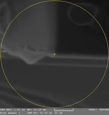
VegaTC: Go to >1000 magnification and move the lower left corner of the sample to the center of the image. This will be defined as the origin of your sample. (If your process involves multiple steps you need to make sure you define the same origin next time.) Make sure to optimize the contrast and brightness of the SEM-image by clicking Gain/Black and then Auto.
E-line: Press , click the Global button (or make sure it is set to Global). Do an Origin Correction (1st tab), click Adjust.
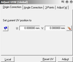
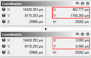
E-line: Note that in the lower-right window, the U and V coordinates change to 0.000, 0.000 µm. The lower left corner of your sample is now defined as the origin of the U/V-coordinate system (as opposed to the X/Y-coordinate system of the stage in general).
¶ Writefield alignment
Because the writing fields (WFs) are spatially limited (typically 100x100 um), we will stitch several WFs to create one pattern. However, in order to properly stitch, we should align the WFs such that their angular and linear offset is zero and their size is all similar. In order to do that, we will perform a WF-alignment procedure on a particle in the little scratch you've made. How well you focus on this particle will determine the resolution of your patterning. With a WF-alignment, the beam coordinate system (U/V) is aligned with the stage coordinate system (X/Y). Without a proper WF-alignment you will get stitch errors at writefield boundaries.
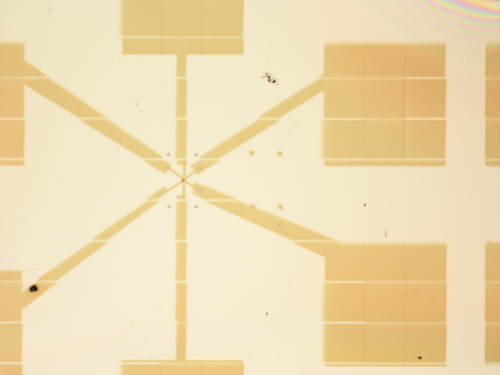
VegaTC: Use the joystick to slowly move upwards from the origin to find the scatch you've made. Follow the scratch all the way to its starting point (i.e. the point closest to the center of your substrate). Do this carefully, as not to accidentally expose parts of the sample. Change the magnification if necessary.
VegaTC: Find a particle which is ~1 µm. The particle is used for focusing and later for automatic alignment procedures. A particle with sharp edges works best. Good particles are small (~1 µm, alone, bright, not in the scratch but next to it (due to the height difference within the scratch)).
Can't find a good particle? When no good particles are present you can create a carbon needle by focusing the beam to one spot. VegaTC:,
Panels/Analysis & Measurement.
VegaTC: Click WD (NOT the checkbox) and vary the working distance. This will (de)focus the particle: find a good focus. By double clicking on the image window, you can use a reduced area, this makes it easier. When you found a good focus: double click Defocus. This will set the defocus to zero, and will allow you to go back easily to your focus.
E-line: Safe the particle position via the Stage Control window, select particle in the menu, click Edit > Read. This is optional, but will allow you to back to the particle easily.
E-line: Set the size of writefields by clicking  . In the upper window, the Writefield Manager, there should be one (or several) WFs available. Make sure you have the correct one selected and press
 ![]() . If you do not know which one is correct, select '2300 x, 100.0 µm': this WF is 100x100 µm, which is the VOF for a magnification of 2300x.
. If you do not know which one is correct, select '2300 x, 100.0 µm': this WF is 100x100 µm, which is the VOF for a magnification of 2300x.
When doing an overlay: First perform a 3-point alignment in Local CS, and then perform a WF alignment.
E-line: In the lower window, the Scan Manager, navigate toward a WF-alignment with a large scan area: Writefield Aligment Procedures > Automatic with Images. Make sure the selected procedure correspond with the current set WF. For 100 µm, this is 100 um WF, Auto ALWF 5 µm marks. Press right click to execute (or drag it in the positionlist).
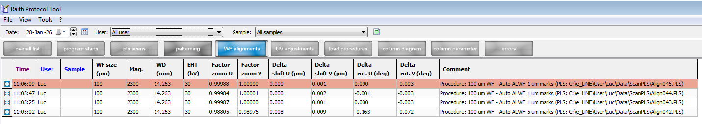
Raith Protocol Tool: Check WF alignment tab and check if parameters for the zoom u/v, shift u/v are in the proper range: zoom u/v = 1,000 ± 0.001 and shift/rotation u/v = ± 0,003 µm.
E-line: Repeat the alignment procedure until the parameters are in the correct range. After the large scan area, you can use the Automatic writefield for smaller areas, e.g. 100 µm WF, 1 µm marks
¶ Exposure parameters
The beam current is used to calculate the exposure time to reach the exposure dose of your resist.
- Measure beam current. It is necessary to measure the beam current again since the filament has to heat up to reach a stable beam current. Optimal filament is achieved after about 60 min. It is recommended to wait about 30 min after starting HV and starting patterning, especially when patterning high resolution structures.
¶ Exposure parameters (II)
Based on the measured beam current and the sensitivity of your resist you can now calculate the exposure parameters.
- E-line/4th tab/click calculator tab
- The goal is to set a specific dose, depending on your design choices and resist type and to have a beam speed that is lower than 15 mm/s.
- Put area dose at 300 µC/cm2 for PMMA 950K. This depends on you resist and you design choices.
- When the tabs are red these parameters are not consistent, this can be resolved by using the calculator buttons next to the parameters
- Set area step size to about 1/3 of your spot size.
- Click ‘calc’ next to area dwell time. If red, add one min area step size. (area size = N * min area step size).
- Line dose should be 3 times area dose (not looking at the units)
- Do not set the beam speed too high, less than 15 mm/s
- Always click ‘calc’ next to dwell time last and make sure the beam speed is not too high
¶ Position list
In the position list you decide what and where to pattern. You can choose the order of patterning and add all sorts of automation scripts.
- E-line/file/new position list, or the
 -button in the toolbar
 - Go to GDSII database, go to your design and drag to position list, select at least one layer, this can be changed later
- Right click 'pattern properties', click 'layer button' and select the layers you want to write in this step
- Set U,V to at least 2,2 (due to imhomogenities in the resist). This will place you pattern at 2,2 mm on your sample.
- Create position matrix if you want to pattern more copies of your device
- Add beamshut down script to the bottom of your positionlist!
- Save your positionlist, especially when doing a proces with multiple steps
¶ Scan
- Check if you didn't forget anything
- You can calculate the time it will take to pattern your device. Patterning parameters/drop down/times.
- Click on scan all in the 'filter' menu to start!
¶ Unloading your sample
- E-line/3rd tab/exchange position and GO
- Check if HV is off (beamshut script should have done this!)
- Vent the chamber
- Unload your sample (GLOVES!)
- Put sample holder in box
- Pump down and check vacuum before you leave
¶ Developing
Each resist typically has a dedicated developer. PMMA type resist can in general be developed by MIBK or a MIBK/IPA solution. See [[resist_and_e-beam_recipes|resist recipes]] for the specific developing process for a specific resist.
¶ Lift off
As for developing, a resist typically has a dedicated remover. Most resists can be removed -lifted off- with aceton. See [[resist_and_e-beam_recipes|resist recipes]] for the specific lift off process for a specific resist.
¶ Overlay
¶ 3-point alignment
- Make sure all previous flags are cleared by unchecking the checkboxes next to the blue flags. (Do not use the blue flags, they have different meaning!)
- 3-point alignment is done to perform a local coordinate system correction. The global markers on the design will be used to line up the local coordinate system of the design with the stage coordinate system.
- Go to faraday cup.
- Open you design. Make sure you are in the viewer and not in the editor, else the flags and stage position will not be shown on your design.
- Open toolbox (T)
- Beware of the meaning of the flags!
- Edit design grid to 1 µm to place the flags accurately, show grid
- Go to the first entry in the (saved!) position list (while your still in global CS), small black triangle in the position list toolbar/go to position.
- Switch to local CS. Xy – uv/local button/3 point tab
- Set the magnification on the SEM to 2300x (Same value as the magnification for the writefield)
- Check with the SEM that you're at the position of the lower left global mark.
- Center the image, make sure the yellow cross sits at the center of the global mark.
- Place 1st flag on the center of the global mark of the lower left corner
- Then click read and then adjust in ‘Adjust UVW (local)’ for P1
- Move to the second global mark, use CTRL-right click in your design to move to the center of the mark.
- Check position in SEM image
- Adjust with the joystick to the center of the global mark
- Set 2nd flag in e-line press read and then adjust
- Do the last flag. It should almost be perfect
- Ctrl-riight in your design, check SEM image, adjust with joystick to center of global mark
- Place 3rd flag
- Press read and then adjust
- Now you have coupled the design coordinates (local coordinates) to the stage coordinates
¶ WF alignment on markers
- After stage alignment, comes e-beam alignment.
- Select an entry in positionlist, right-click to go to properties
- Select layers, only automatic marks, layer 61
- Select as working area WF calibration.
- Click ‘position button’ (Since we are now in local CS (design CS) you do not select the coordinates where your device will be patterned) the coordinates will be calculated from the working area you selected.
- Go to your position and click execute (F9)
- Run the WF calibration a few times until the parameters are correct in Raith Protocol Tool.
- When you want to start the patterning, select layers you want to pattern, choose the working area and click the position button.
- SCAN all to start the patterning.
¶ Tips and tricks
¶ AUTO HEAT
Move the stage to a empty part of the waferholder. Turn on the beam and make sure focus is good.
Press 'AUTO' next to 'HEAT' in VegaTC.
The system will find the optimal saturation point for heating of the filament and will perform an auto gun alignment. Check if the gun tilt and gun shift values are between -20% and 20%. If the values are 0% this means the procedure failed. To high values need be adjusted with a mechanical alignment of the filament, find a technician to do this for you.
¶ Switching PC
Often it is necessary to switch to a lower PC to write large structures. PC-1 has a 700nm spot size, compared to a 70nm spot size for PC-10. FIXME Writing large structures >1µm, can be done with a high PC, but will require long patterning times.\
Since the spot size of PC1 is large, the resolution to do a proper writefield alignment is low. For this reason the PC is changed after the writefield alignment is performed at PC-10, but before the beam current is measured. Switching between PC generally introduces a small shift in the pattern. When you take into account this error during the design of your pattern you can easily correct for the shift without going through the trouble of a proper writefield alignment for a low PC.
¶ Keyboard shortcuts
¶ E-line
| Hotkey | Function |
|---|---|
| L | shows the layer information of your design |
| W | shows working area information of your design |
| H | selects the handtool to move around on the design |
| T | opens the toolbox |
¶ Vega-TC
Double click to create a reduced area in the SEM image. When reduced area is active you can change the size of the area using the right mouse button.
¶ Common problems
¶ Failed WF alignment
A failed WF alignment typically happens when a particle isn't anymore in the field of view (FoV) of the WF alignment procedure. This indicates the parameters have drifted from the optimal settings after a -few- bad WF alignments. A bad WF aligment can be due to: bad focus, WF alignment at low PCs (low resolution), particle not centred, etc...\
In the second tab 'writefield' control, open 'writefield manager', reset the WF alignment. Choose a WF alignment with large FoV (> 10µm). After this rough WF alignment reset the shift values in the writefield manager. Then perform the WF alignment you need till you're happy with the correction values in Raith Protocol Tool.
¶ Extra reading
{{ :fundamentals_of_electron_beam_exposure_and_development.pdf|}}